- 您现在的位置:买卖IC网 > Sheet目录346 > NCV8855BMNR2GEVB (ON Semiconductor)BOARD EVALUATION NCV8855 ASIC
�� �
�
�NCV8855�
�I� D(avg)� +� IOUT2� 1� *�
�VOUT2�
�D� VOUT� ESR� +� D� IOUT�
�(� D� IOUT)�
�L�
�VIN� min� D� MAX� *� VOUT�
�dI� L� V� L�
�Inductor� Slew� Rate� +�
�+�
�SMPS2� Diode� Selection�
�The� diode� in� SMPS2� provides� the� inductor� current� path�
�when� the� power� switch� turns� off.� This� is� known� as� the�
�non� ?� synchronous� diode� or� commutation� diode.� The� peak�
�reverse� voltage� is� equal� to� the� maximum� operating� input�
�voltage.� The� peak� conducting� current� is� determined� by� the�
�internal� current� limit.� The� average� current� can� be� calculated�
�from:�
�(eq.� 10)�
�VIN_SW�
�However,� the� worse� case� diode� average� current� occurs�
�during� a� short� circuit� condition.� For� a� diode� to� survive� an�
�indefinite� short� circuit� condition,� the� current� rating� of� the�
�diode� should� be� equal� to� the� maximum� current� limit� which�
�is� 3.6� A.� Thus� the� MBRS4201T3� is� the� diode� of� choice.�
�Inductor� Selection�
�Both� mechanical� and� electrical� considerations� influence�
�the� selection� of� an� output� inductor.� From� a� mechanical�
�perspective,� smaller� inductor� values� generally� correspond� to�
�smaller� physical� size.� Since� the� inductor� is� often� one� of� the�
�largest� components� in� SMPS� system,� a� minimum� inductor�
�value� is� particularly� important� in� space� ?� constrained�
�applications.� From� an� electrical� perspective,� smaller�
�inductor� values� correspond� to� faster� transient� response.� The�
�maximum� current� slew� rate� through� the� output� inductor� for�
�a� buck� regulator� is� given� by:�
�(eq.� 11)�
�dt� L�
�Where� I� L� is� the� inductor� current,� L� is� the� output�
�inductance,� and� V� L� is� the� voltage� drop� across� the� inductor.�
�This� equation� indicates� that� larger� inductor� values� limit� the�
�regulator� ’s� ability� to� slew� current� through� the� output�
�inductor� in� response� to� output� load� transients.� Consequently,�
�output� capacitors� must� supply� (or� store)� sufficient� charge� to�
�maintain� regulation� while� the� inductor� current� “catches� up”�
�to� the� load.� This� results� in� larger� values� of� output� capacitance�
�to� maintain� tight� output� voltage� regulation.�
�In� contrast,� smaller� values� of� inductance� increase� the�
�SMPS� Output� Capacitor� Selection�
�The� output� capacitor� is� a� basic� component� for� the� fast�
�response� of� the� power� supply.� In� fact,� during� load� transient,�
�for� first� few� microseconds� they� supply� the� current� to� the�
�load.� The� controller� recognizes� the� load� transient� and�
�proceeds� to� increase� the� duty� cycle� to� its� maximum.�
�Neglecting� the� effect� of� the� ESL,� the� output� voltage� has� a�
�first� drop� due� to� the� ESR� of� the� bulk� capacitor(s).�
�ESR� (eq.� 13)�
�A� lower� ESR� produces� a� lower� D� V� during� load� transient.�
�In� addition,� a� lower� ESR� produces� a� lower� output� voltage�
�ripple.�
�The� voltage� drop� due� to� the� output� capacitor� discharge� can�
�be� approximated� using� the� following� equation:�
�2�
�D� VOUT� discharge� +�
�2� COUT�
�(eq.� 14)�
�where,� D� MAX� is� the� maximum� duty� cycle� value,� which� is�
�90%.� Although� the� ESR� effect� is� not� in� phase� with� the�
�discharging� of� the� output� voltage,� D� VOUT� (ESR)� can� be�
�added� to� D� VOUT� (discharge)� to� give� a� rough� indication� of� the�
�maximum� D� VOUT� during� a� transient� condition.� Simulation�
�can� also� help� determine� the� maximum� D� VOUT;� however,� it�
�will� ultimately� have� to� be� verified� with� the� actual� load� since�
�the� ESL� effect� is� dependent� on� layout� and� the� actual� load’s�
�di/dt.�
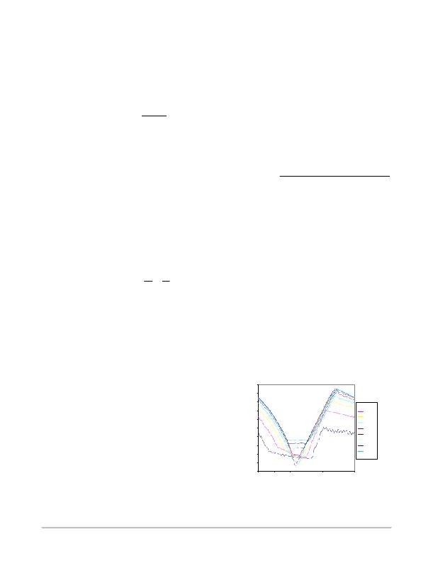
�SMPS� Input� Capacitor� Selection�
�The� primary� consideration� for� selecting� the� input�
�capacitor� is� input� RMS� current.� However,� since� there� are�
�two� SMPS� running� out� ?� of� ?� phase� with� each� other,�
�calculating� the� input� RMS� current� can� be� complicated.� The�
�graphs� below� shows� how� the� input� RMS� current� is� affected�
�by� differing� phase� angles� between� SMPS1� and� SMPS2.� The�
�plot� below� was� generated� with� VOUT1� at� 5� V� with� a� load� of�
�2� A� and� an� output� inductor� value� of� 10� m� H,� and� VOUT2� at�
�8� V� with� a� load� of� 4� A� and� an� output� inductor� value� of� 10� m� H.�
�VOUT� VOUT�
�I� PP� +� FSW�
�1� *�
�regulator� ’s� maximum� achievable� slew� rate� and� decrease� the�
�necessary� capacitance,� at� the� expense� of� higher� ripple�
�current.�
�In� continuous� conduction� mode,� the� peak� ?� to� ?� peak� ripple�
�current� is� calculated� using� the� following� equation:�
�(eq.� 12)�
�L� VBATT�
�From� this� equation� it� is� clear� that� the� ripple� current�
�increases� as� L� decreases,� emphasizing� the� trade� ?� off� between�
�dynamic� response� and� ripple� current.�
�For� most� applications,� the� inductor� value� falls� in� the� range�
�between� 2.2� m� H� and� 22� m� H.� There� are� many� magnetic�
�component� vendors� providing� standard� product�
�3.00�
�2.80�
�2.60�
�2.40�
�2.20�
�2.00�
�1.80�
�1.60�
�1.40�
�1.20�
�1.00�
�0.00�
�60.00�
�120.00� 180.00� 240.00� 300.00� 360.00�
�Phase� (VOUT1� vs� VOUT2)�
�9.00�
�10.00�
�11.00�
�12.00�
�13.00�
�14.00�
�15.00�
�16.00�
�17.00�
�18.00�
�lines� suitable� for� SMPS1� and� SMPS2’s� requirements.�
�TDK� offers� the� RLF12545� ?� PF� series� inductors,� which� are�
�recommended� for� the� automotive� radio� application.�
�http://onsemi.com�
�19�
�Figure� 22.� Irms� vs� Phase�
�发布紧急采购,3分钟左右您将得到回复。
相关PDF资料
NCV8871BSTGEVB
BOARD EVAL NCV8871BST BOOST CTLR
NHC-14150
VALULINE 8" X 8.5" X 1.75"
NHC-14151
VALULINE 8" X 17" X 1.75"
NHC-14152
VALULINE 13" X 17" X 1.75"
NHC-14153
VALULINE 8" X 8.5" X 3.5"
NHC-14154
VALULINE 8" X 17" X 3.5"
NHC-14155
VALULINE 13" X 17" X 3.5"
NHC-14156
VALULINE 13" X 17" X 5.25"
相关代理商/技术参数
NCV8870
制造商:ONSEMI 制造商全称:ON Semiconductor 功能描述:Automotive Grade Non-Synchronous Boost Controller
NCV887000
制造商:ONSEMI 制造商全称:ON Semiconductor 功能描述:Automotive Grade Non-Synchronous Boost Controller
NCV887000D1R2G
功能描述:低压差稳压器 - LDO Auto Grade Non-Sync Boost Controller
RoHS:否 制造商:Texas Instruments 最大输入电压:36 V 输出电压:1.4 V to 20.5 V 回动电压(最大值):307 mV 输出电流:1 A 负载调节:0.3 % 输出端数量: 输出类型:Fixed 最大工作温度:+ 125 C 安装风格:SMD/SMT 封装 / 箱体:VQFN-20
NCV887001
制造商:ONSEMI 制造商全称:ON Semiconductor 功能描述:Automotive Grade Non-Synchronous Boost Controller
NCV887001D1R2G
功能描述:低压差稳压器 - LDO Auto Grade Non-Sync Boost Controller
RoHS:否 制造商:Texas Instruments 最大输入电压:36 V 输出电压:1.4 V to 20.5 V 回动电压(最大值):307 mV 输出电流:1 A 负载调节:0.3 % 输出端数量: 输出类型:Fixed 最大工作温度:+ 125 C 安装风格:SMD/SMT 封装 / 箱体:VQFN-20
NCV887100D1R2G
功能描述:DC/DC 开关控制器 AUTOMOTIVE-GRADE NON-SYNC RoHS:否 制造商:Texas Instruments 输入电压:6 V to 100 V 开关频率: 输出电压:1.215 V to 80 V 输出电流:3.5 A 输出端数量:1 最大工作温度:+ 125 C 安装风格: 封装 / 箱体:CPAK
NCV887101D1R2G
功能描述:IC REG CTRLR BST PWM CM 8-SOIC RoHS:是 类别:集成电路 (IC) >> PMIC - 稳压器 - DC DC 切换控制器 系列:- 产品培训模块:Lead (SnPb) Finish for COTS
Obsolescence Mitigation Program 标准包装:2,500 系列:- PWM 型:电流模式 输出数:1 频率 - 最大:275kHz 占空比:50% 电源电压:18 V ~ 110 V 降压:无 升压:无 回扫:无 反相:无 倍增器:无 除法器:无 Cuk:无 隔离:是 工作温度:-40°C ~ 85°C 封装/外壳:8-SOIC(0.154",3.90mm 宽) 包装:带卷 (TR)
NCV887102D1R2G
功能描述:IC REG CTRLR BST PWM CM 8-SOIC RoHS:是 类别:集成电路 (IC) >> PMIC - 稳压器 - DC DC 切换控制器 系列:- 产品培训模块:Lead (SnPb) Finish for COTS
Obsolescence Mitigation Program 标准包装:2,500 系列:- PWM 型:电流模式 输出数:1 频率 - 最大:275kHz 占空比:50% 电源电压:18 V ~ 110 V 降压:无 升压:无 回扫:无 反相:无 倍增器:无 除法器:无 Cuk:无 隔离:是 工作温度:-40°C ~ 85°C 封装/外壳:8-SOIC(0.154",3.90mm 宽) 包装:带卷 (TR)